Image sensor promotes the development of embedded vision technology

Image sensor promotes the development of embedded vision technology

New imaging applications are booming, from collaborative robots in Industry 4.0 to drone firefighting or for agriculture, to biometric facial recognition, to handheld medical devices at home. A key factor in the emergence of these new applications is that embedded vision is more pervasive than ever. Embedded vision is not a new concept; it simply defines a system that includes a visual setup that controls and processes data without an external computer. It has been widely used in industrial quality control, and familiar examples such as "smart cameras."
In recent years, the development of hardware devices for the consumer market economy has resulted in a significant reduction in bill of materials (BOM) costs and product size compared to previous computer-based solutions. For example, small system integrators or OEMs can now purchase SVI or module systems such as NVIDIA Jetson in small quantities; larger OEMs can directly obtain Qualcomm Snapdragon or Intel Movidius Myriad. 2 and so on image signal processor. At the software level, the market software library can speed up the development of dedicated vision systems and reduce the difficulty of configuration, even for small batch production.
The second change that drives the development of embedded vision systems is the emergence of machine learning, which enables the neural network in the lab to be trained and then uploaded directly to the processor so that it can automatically identify features and make decisions in real time.
Being able to offer solutions for embedded vision systems is critical for imaging companies looking for these high-growth applications. Image sensors have an important role in large-scale introduction because they can directly affect the performance and design of embedded vision systems. The main driving factors can be summarized as: smaller size, weight, power consumption and cost. SWaP-C" (decreasing Size, Weight, Power and Cost).
1. Reducing costs is critical
Acceleration pushers for new embedded vision applications are priced to meet market demands, and vision system costs are a major constraint in achieving this requirement.
1.1 . Saving optical costs
The first way to reduce the cost of the vision module is to reduce the size of the product for two reasons: first, the smaller the pixel size of the image sensor, the more chips can be fabricated on the wafer; on the other hand, the sensor can be used smaller and lower. Cost optical components, both of which can reduce the inherent cost. For example, the Eledald 5M sensor from Teledyne e2v reduces the pixel size to 2.8μm, allowing the S-port (M12) lens to be used on a five-megapixel global shutter sensor, resulting in direct cost savings – the price of an entry-level M12 lens It's about $10, and the larger C- or F-port lens costs 10 to 20 times. So reducing size is an effective way to reduce the cost of embedded vision systems.
For image sensor manufacturers, this reduced optical cost has another impact on the design because, in general, the lower the optical cost, the less ideal the incident angle of the sensor. Therefore, low cost optics require the design of specific displacement microlenses over the pixels to compensate for distortion and focused light from the wide angle.
1.2. Sensor low cost interface
In addition to optical optimization, the choice of sensor interface also indirectly affects the cost of the vision system. The MIPI CSI-2 interface is the right choice for cost savings (it was developed by the MIPI Alliance for the mobile industry). It has been widely adopted by most ISPs and has begun to be adopted in the industrial market because it provides a low-cost system-on-a-chip (SOC) or system-on-a-system (SOM) from companies such as NXP, Nvidia, Qualcomm or Intel. integrated. Design a CMOS image sensor with MIPI CSI-2 sensor interface, without any intermediate converter bridge, directly transfer image sensor data to the host system SOC or SOM of the embedded system, saving cost and PCB space, of course, This advantage is even more pronounced in multi-sensor based embedded systems such as the 360 ​​degree panoramic system.
However, these benefits are limited because the MIPI interface's connection distance is limited to 20 cm, which may not be ideal in remote settings where the sensor is far from the host processor. In these configurations, a camera board solution with an integrated longer interface is a good choice at the expense of miniaturization. Some off-the-shelf solutions can be integrated. For example, camera boards from industrial camera manufacturers (such as Flir, AVT, Basler, etc.) can usually be used in MIPI or USB3 interfaces, which can reach a range of more than 3 meters to 5 meters.
1.3. Reduce development costs
Increasing development costs are often a challenge when investing in new products; it can cost millions of dollars in one-time development costs and put pressure on time to market. For embedded vision, this pressure becomes even greater, because modularity (ie, whether the product can switch to multiple image sensors) is an important consideration for integrators. Fortunately, by providing a degree of cross-compatibility between sensors, for example, by defining a family of components that share the same pixel architecture to have stable optoelectronic performance, sharing a single front-end mechanism with a shared optical center, and being compatible PCB components to simplify evaluation, integration and supply chain, thereby reducing development costs.
To simplify the design of the camera board (even for a variety of sensors), there are two ways to design a sensor package. Pin-to-pin compatibility is the choice of camera board designers because it enables multiple sensors to share the same circuitry and control, making assembly completely unaffected by PCB design. Another option is to use size-compatible sensors so that multiple sensors can be used on the same PCB, but this also means they may have to deal with the differences in the interface and wiring of each sensor.
2. Energy efficiency provides better individual work ability
Micro-battery-driven devices are clearly benefiting from embedded vision applications because external computers prevent any portable applications from happening. To reduce system power consumption, image sensors now include a variety of features that enable system designers to save power.
From a sensor perspective, there are several ways to reduce the power consumption of the embedded vision system without compromising the acquisition frame rate. The simple approach is to minimize the dynamic operation of the sensor itself at the system level by using standby or idle mode for as long as possible. Standby mode reduces the power consumption of the sensor to less than 10% of the operating mode by turning off the emulation circuit. The idle mode halved the power consumption and allowed the sensor to restart the acquisition of the image in microseconds.
Another way to integrate energy savings in sensor design is to use advanced lithography node technology. The smaller the technology node, the smaller the voltage required to convert the transistor, and the power consumption is proportional to the voltage, which reduces power consumption. So the pixel produced using 180nm technology 10 years ago not only reduced the transistor to 110nm, but also reduced the voltage of the digital circuit from 1.9 volts to 1.2 volts. The next generation of sensors will use 65nm technology nodes, making embedded vision applications more energy efficient.
The last point is that by choosing the right image sensor, the energy consumption of the LED can be reduced under certain conditions. Some systems must use active illumination, such as three-dimensional map generation, motion pauses, or purely sequential pulses to specify the wavelength to increase contrast. In these cases, reducing the noise of the image sensor in low-light environments can achieve lower power consumption. By reducing sensor noise, engineers can decide to reduce the current density intensity or reduce the number of LEDs integrated into the embedded vision system. In other cases, when image capture and LED flicker are triggered by an external event, selecting the appropriate sensor readout structure can significantly save power. With traditional rolling shutter sensors, the LEDs must be fully open for full frame exposure, while the global shutter sensor allows LEDs to be turned on only in certain parts of the frame. So if you use an intra-pixel correlated double sampling (CDS) application, replacing the rolling shutter sensor with a global shutter sensor saves on lighting costs while still maintaining the same low noise as the CCD sensor used in the microscope.
3. On-chip functionality paves the way for visual systems designed for applications
Some of the directional extension concepts of embedded vision led us to fully customize the image sensor to integrate all processing functions (system on the chip) in 3D stacking to optimize performance and power consumption. However, the cost of developing such a product is very high, and it is not entirely impossible in the long run to be able to achieve this level of integrated sensor. Now we are in a transitional phase, including embedding some functions directly into the sensor to Reduce computational load and speed up processing time.
For example, in bar code reading applications, Teledyne e2v has patented technology that incorporates an embedded function that includes a proprietary barcode recognition algorithm into the sensor chip. This algorithm can find the position of the barcode within each frame and let the image signal processor Just focus on these ranges and improve data processing efficiency.
Figure 2: Teledyne e2v Snappy 5 megapixel chip that automatically recognizes barcode position
Another feature that reduces processing load and optimizes "good" data is Teledyne E2V's patented fast exposure mode, which allows the sensor to automatically correct exposure time to avoid saturation when lighting conditions change. This feature optimizes processing time because it accommodates fluctuations in illumination in a single frame, and this fast response reduces the number of "bad" images that the processor needs to process.
These features are usually specific and require a good understanding of the client's application. As long as you have a good understanding of the application, you can design a variety of other on-chip features to optimize the embedded vision system.
4. Reduce the weight to match the minimum application space
Another major requirement for embedded vision systems is the ability to fit tight spaces or to be small enough to be used in handheld devices and/or to extend battery-operated product hours. This is why most embedded vision systems now use low resolution small optical format sensors with only 1MP to 5MP.
Reducing the size of the pixel chip is only the first step in reducing the footprint and weight of the image sensor. The current 65nm process allows us to reduce the global shutter pixel size to 2.5μm without compromising optoelectronic performance. This manufacturing process enables a full HD global shutter CMOS image sensor to meet the requirements of the mobile phone market with less than 1/3 inch size.
Another major technique to reduce sensor weight and footprint is to shrink the package size. Chip-scale packaging has grown rapidly in the market over the past few years and is particularly evident in mobile, automotive electronics and medical applications. Compared to the traditional ceramic (Ceramic Land Grid Array, CLGA for short) package commonly used in the industrial market, the chip-scale fan-out package enables higher density connections, making it an excellent solution for the lightweight and miniaturized challenges of embedded system image sensors. For example, Teledyne e2v's Emerald 2M image sensor chip scale package, the side height is only half of the ceramic package, and the size is reduced by 30%.
Looking ahead, we expect new technologies to further enable the smaller sensor sizes required for embedded vision systems.
The 3D stack is an innovative technology for the production of semiconductor devices. Its principle is to fabricate various circuit chips on different wafers, and then stack and interconnect them using copper-to-copper connections and through silicon vias (TSV) technology. . The three-dimensional stack allows the device to achieve a smaller footprint than conventional sensors because it is a multi-layer stacked chip. In a three-dimensional stacked sensor, the read and processing chips can be placed below the pixel chip and the row decoder. Thus, the footprint size of the sensor is reduced by the reduced readout and processing chips, and more processing resources can be added to the sensor to reduce the load on the image signal processor.
However, to make 3D stack technology widely used in the image sensor market, there are still some challenges. First of all, this is an emerging technology, followed by its higher cost, because additional process steps are required, making the chip cost more than three times higher than chips using conventional technology. Because 3D burying will be primarily a choice of embedded vision systems with high performance or very small footprint.
In summary, the embedded vision system can be summarized as a "lightweight" vision technology that can be used by different types of companies including OEMs, system integrators, and standard camera manufacturers. "Embedded" is a general description that can be used for different applications, so it is not possible to open a list to illustrate its characteristics. However, there are several applicable rules for optimizing embedded vision systems. In general, the market driving force is not from super fast speed or super high sensitivity, but size, weight, power consumption and cost. Image sensors are the main driver of these conditions, so careful selection of appropriate image sensors is needed to optimize the overall performance of the embedded vision system. A suitable image sensor provides more flexibility for embedded designers, saving bill of materials costs and reducing the footprint of lighting and optical components. It also allows designers to choose from a large number of affordable image signal processors from the consumer market that have optimized deep learning capabilities without the need for more complexity.

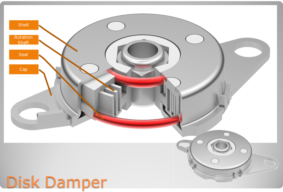
Flat disk Rotary Damper mainly used for large diameter, small height space. Disk dampers provide energy absorption and rotational deceleration. We offer many different models from mild to extreme. Our disk dampers are the perfect solution for a wide range of applications, from scanner, and glove boxes to auditorium seating to. Disk dampers are designed to control and smooth out the opening and closing of lids, and doors.

Our damper is conducive to performing structural movement in soft, silent and safe environment, mitigating impact load, avoiding strike damage, prolonging mechanical life, reducing noise disturbance, improving product quality and improve customer satisfaction.


Anatomy of the Disk Damper


NOTE:
1. Please contact the corresponding product engineer for specific torque products. 
2. Max. rotation speed: 50r/min
3. Max. circle rate: 6 cycle/min ( Clockwise360 °, 360 ° anti-clockwise for 1 cycle)
4. Operating temperature: -10~50℃
5. Storage temperature:-30~80℃

  NO. Description Material
1 Shell SPFC
2 Cover SPFC
3 Shaft PA/POM
Disk Damper


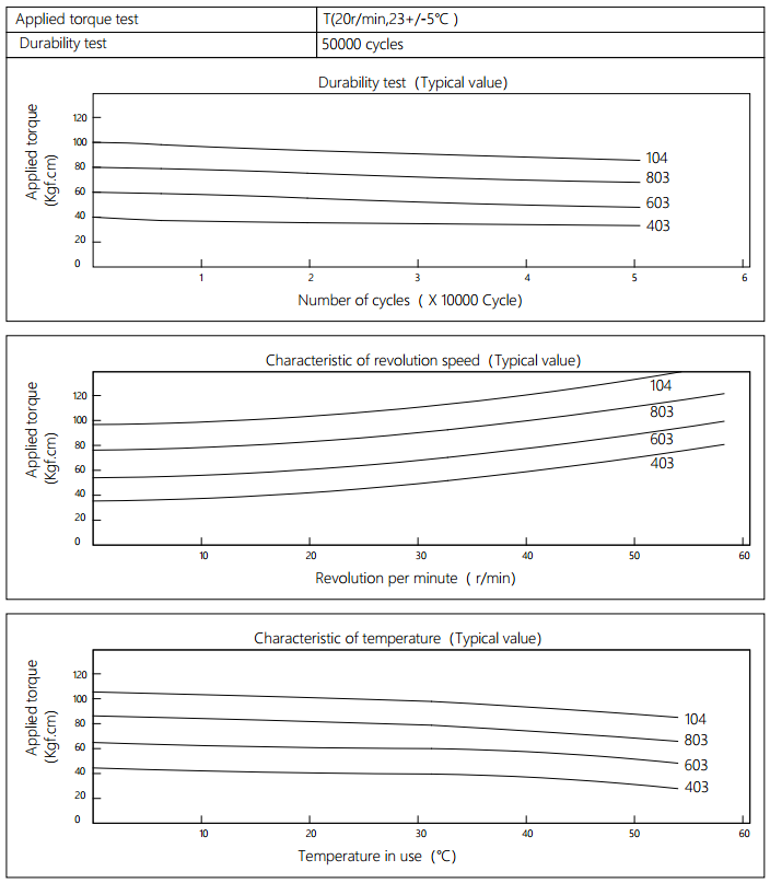
Disk Damper Characteristics

Applied torque:(T)
Test Temperature: 23+/-5℃
Rotating speed: 20r/min
Durability test Metho: Clockwise 360 °, 360 °anti-clockwise
Rotating speed: 20r/min
Test Frequency: (1cycle/min)
Test Temperature: 23±5℃
Durability test cycle: 50000 cycle
Test result criteria: Store in the room temperature for 24 hours or more after the test, recording to the torque T=T±30%T.
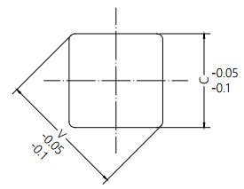
Disk Damper Square Hole


The damper square hole coordinateswith the rotation axis dimension tolerance.


Disk Damper

Disk Damper,Adjustable Dampers,Excavator Disk Damper,Spare Disk Damper,Oval Disk Damper

Shenzhen ABD Equipment Co., Ltd. , https://www.abddamper.com