Double Flanged Ball Valve,Flanged Ball Valve,Cast Iron Flanged Valve Doctech Auto-Control Valve Co., Ltd. , http://www.twtvalves.com
There are four ways to measure RF power:
1 using diode detection power method;
2 equivalent thermal power detection method;
3 True RMS> DC (TRMS> DC) conversion detection power method;
4 logarithmic amplification detection power method. These four methods are introduced separately and their advantages and disadvantages are compared. Finally, the optimal design of the RF power measurement system is described.
1, using diode detection power method diode detection input power circuit shown in Figure 1 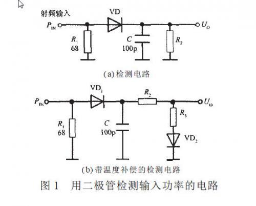
Figure 1(a) shows a simple half-wave rectification and filtering circuit with a total input resistance of 50Ω. VD is a rectifier and C is a filter capacitor. After the RF input power PIN is rectified and filtered, the output voltage UO is obtained. However, when the ambient temperature increases or decreases, the UO decreases significantly. Figure 1 (b) is a modified diode detection input power circuit, the circuit adds a temperature compensation diode VD2, diode VD1 rectified voltage temperature compensation. The diode has a negative temperature coefficient. When the temperature rises, the voltage drop of VD1 decreases, but the voltage drop of VD2 also decreases. Finally, the output voltage remains constant. The characteristic curves of UO and PIN and the error γ after compensation are shown in Fig. 2. Fig. 2 shows the error curves when the ambient temperature is +25°C, -40°C and +85°C, respectively.
It should be pointed out that the diode detection circuit responds with the average value. It cannot directly measure the effective value of the input power, but indirectly measures the RMS power according to the relationship between the RMS value of the sine wave and the average value. Obviously, when the measured waveform is not a sine wave, the crest factor is not equal to 1.4142, which will produce a larger measurement error. 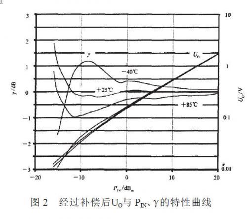
2. Equivalent thermal power detection method The equivalent thermal power detection method is based on the second definition of the effective value, and its detection circuit is shown in FIG. 3 . It compares the effective heat of an unknown AC signal with the effective heat of a DC reference voltage. When the temperature difference between the signal resistor (R1) and the reference resistor (R2) is zero, the power consumption of the two resistors is equal, so the effective value of the unknown signal voltage is equal to the effective value of the DC reference voltage. R1 and R2 are matching resistors, and all use low-temperature-coefficient resistors. The voltage drop between them is kUI and kUO. In order to measure the temperature difference, there are voltage output type temperature sensors A and B in the vicinity of R1 and R2, respectively. Two thermocouples are used to measure the temperature difference. The overheat protection resistors are also connected in series on R1 and R2, respectively. 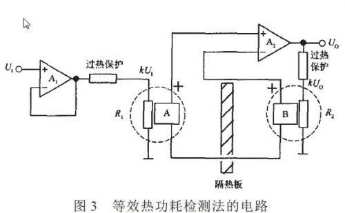
Although the principle of the equivalent thermal power detection method is very simple, it is difficult to achieve in practical applications, and the price of such testing equipment is very expensive.
3, True rms / DC (TRMS / DC) conversion detection power law true RMS E DC conversion detection power method is the biggest advantage is that the measurement results and measured signal waveform has nothing to do, this is the "true RMS" meaning. Therefore, it can accurately measure the true rms power of an arbitrary waveform. The first method of measuring true rms power is to use a monolithic rms DC converter (such as the AD636 model) that first measures the true rms voltage level and then converts it to its true rms power level.
Another circuit diagram for measuring true rms power is shown in Figure 4. The typical product for this circuit is the AD8361 monolithic RF rms power detection system IC. UI is the RF signal input terminal, and UO is the DC voltage output terminal. The US is terminated with a +2.7V to +5.5V power supply, and COM is a public ground. IREF is the reference end of the reference mode and PWDN is the sleep mode control end. The FLTR is the filter terminal. A capacitor is connected in parallel between the terminal and the US terminal to reduce the cutoff frequency of the filter. SREF is the power reference control terminal. 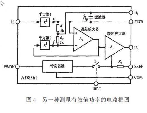
The radio frequency rms voltage input from the UI terminal is UI. After passing through the squarer 1, a pulsating current signal i proportional to UI2 is generated. The current signal passes through a square law detector composed of an internal resistor R1 and a capacitor C to obtain a mean square value voltage. UI2, input to the non-inverting input of the error amplifier. Using a squarer 2 and an error amplifier can form a closed negative feedback circuit and add the negative feedback signal to the inverting input of the error amplifier for temperature compensation. When the closed-loop circuit reaches a steady state, the output voltage UO(DC) is proportional to the input power value PIN. There is relation UO=kPIN(1)
Where k is the output voltage sensitivity of a true rms DC converter, k = 7.5mV/dBm for the AD8361. This detection method has the following advantages: (1) Since the two squarers are identical, they are not Impact on conversion accuracy;
(2) When the ambient temperature changes, the two squarers can compensate each Other to keep the output voltage stable;
(3) The frequency band of the squarer used is very wide, from DC to microwave frequency band.
4, logarithmic amplification detection power law logarithmic amplification detector is composed of multi-stage logarithmic amplifier, the circuit block diagram shown in Figure 5. 
There are 5 logarithmic amplifiers (AE) in Figure 5, each with a gain of 20dB (ie, a 10x voltage amplification factor), and the maximum output voltage is limited to 1V. Therefore, the slope of the logarithmic amplifier kS =1V/20dB=50mV/dB. The output voltages of the 5 logarithmic amplifiers are sent to the summation unit (Σ) through the detector, and the output voltage UO is obtained through the low-pass filter. The logarithmic amplifier can input AC signals. Envelope logarithm operation, the output voltage and kS, PIN relationship formula UO = kS (PIN-b) (2)
Where b represents the intercept, which corresponds to the input power level value when the output voltage is zero.
The characteristic of ordinary logarithmic amplifiers applies only to sine wave input signals. When the input signal is not a sine wave, the intercept on the characteristic curve will change, affecting the output voltage value. At this point, the output reading should be corrected. It should be pointed out that although the AD8362 monolithic RF rms power detector manufactured by Analog Devices is also a logarithmic detection power method, it can be applied to any input signal waveform by using a unique patented technology, and the intercept on the characteristic curve Does not change with the input signal.
5, the optimal design of the radio frequency power detection system The circuit of the traditional radio frequency power meter or radio frequency detection system is complicated, the integration degree is very low. Recently, Analog Devices Inc. has introduced the AD8361, AD8362, and AD8318 fully integrated monolithic RF rms power detectors to accurately measure RF power as well as IF and LF power. . In addition, Linear Technology of the United States has also developed the LT5504, LTC5507 monolithic RF power detectors. The advent of this kind of chip has created the conditions for the optimal design of RF and broadband true RMS power detection systems. The main performance indicators of the four single-chip RF power detectors are shown in Table 1. 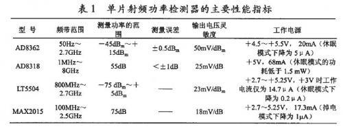
The circuit formed by the AD8318 RF power controller is shown in Figure 6. 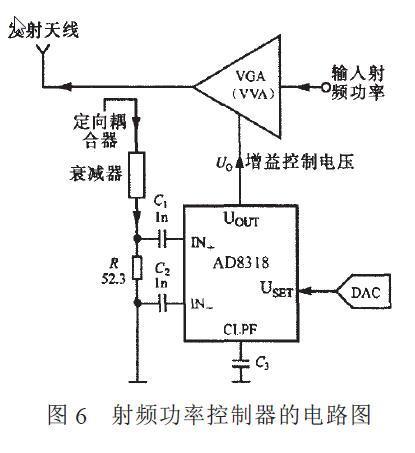
The control object may be a power amplifier (PA), a variable gain amplifier (VGA), a variable voltage attenuator (VVA), or the like. When selecting the control mode, disconnect the USET and UOUT pins from each other. The measured RF power signal is applied to the input of the AD8318 through a directional coupler and attenuator. The set voltage of the AD8318 is taken from a digital-to-analog converter (DAC). The gain control voltage output from the UOUT of the AD8318 is used to control the output power of the VGA (or VVA).
RF Power Measurement Technology and Its Application
Introduction The RF power meter is generally composed of a power sensor (also called a power probe), a power detection circuit, and a display device. Power score absorption (also known as terminal type) and through the two, the former is the power sensor probe as the terminal load of the system under test, from which it absorbs all measured power, and finally through the display shows the measured power value.